Sandwich-Like Superlattice Structures Provide New Insight Into Materials Design
To improve scientific understanding of materials design, and to pave the way for faster, thinner and more efficient electronics, scientists around the world are working to exploit the novel electronic properties of quantum materials. One approach is to design new systems, not found in nature, by creating superlattices: atomically precise stacks of alternating atomic layers of different materials. These superlattice structures are, in essence, ‘sandwiches’ made of layers just a few atoms thick, with each layer composed of arrays of interfaces between different materials. As Herbert Kroemer, who received the Nobel Prize in physics in 2000 for his work on the semiconductor superlattices that underlie modern computer technology, once observed: “The interface is the device.”
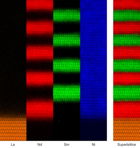
In a paper published recently in Nature Materials, the theorists Alex Georgescu, Antoine Georges and Andrew Millis of the Flatiron Institute’s Center for Computational Quantum Physics in New York City, together with Alain Mercy, Yajun Zhang and Philippe Ghosez of the University of Liège, joined the experimentalists Claribel Dominguez, Jennifer Fowlie, Adrien Waelchli and Sara Catalano from Jean-Marc Triscone’s group at the University of Geneva, as well as Bernat Mundet and Duncan Alexander of the École Polytechnique Fédérale de Lausanne (EPFL) in Switzerland and Marta Gibert of ETH Zurich. Together, they report on a novel interfacial effect that can be used to achieve fine control over the electronic properties of an artificially layered nickelate material.
Nickelates are transition metal oxides, a family of materials that may eventually replace silicon-based technology in everyday electronics. At high temperatures, nickelates are metals. But as the temperature decreases below a critical value, they abruptly become insulators. As a nickelate is tuned across this insulator-metal transition, its conductivity can decrease significantly — up to 1 million times. The physics of the metal-insulator transition is a central topic in modern condensed matter physics and is highly appealing for its potential in energy-efficient electronic applications including piezo-transistors and memristors.
Fascinatingly, the metal-insulator transition temperature can be engineered with high precision. How? Nickelate crystals are composed of nickel, oxygen and another so-called rare earth ion. It turns out that substituting different rare earth ions changes the nickelate’s bond angles and bond lengths, allowing the metal-insulator transition to be tuned from over 572 F (300 C) down to absolute zero.
In the Nature Materials study, the research team used artificial materials that were made in Geneva. The materials are comprised of alternating layers of two nickelates with different rare earths. This results in two different metal-insulator transition temperatures: one at 270 F (130 C) and the other at −100 F (−73 C). When the layers are thick, the superlattice behaves as a composite of two materials with separate metal-insulator transitions. But if the layers are thinner — for example, less than eight atoms per layer — then the whole structure behaves like a brand-new material with a single transition at an intermediate temperature.
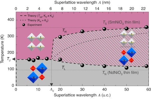
How do we pinpoint the critical thickness needed to create this new material? The previously accepted view was that it all came down to structure. In these picoscale-engineered systems, compounds stack on top of each other perfectly, so that the different levels of distortion must match smoothly at the interfaces and then decay away from them. The resulting spatial pattern of the atomic distortions was believed to uniquely define the electronic properties of the new artificial material.
However, the researchers behind the Nature Materials paper found this not to be the case. When Mundet of the EPFL team performed advanced scanning transmission electron microscopy experiments, supported by sophisticated calculations from the New York and Liège teams, the combined results showed that the distortions do indeed change smoothly across the interfaces. Crucially, these distortions revert to the homogeneous material values within one- to- two atomic planes of the interface. This means that distortion matching cannot explain the unique metal-insulator transition observed when the layers are thicker than one or two atomic planes, and certainly not when they are up to eight atoms thick.
If it is not crystal structure, what tells a material that it is coupled to a nearby layer of a different material? The research team found that the coupling comes from the electronic and structural energy cost of an interface between a metallic region and an insulating one. If the layers are too thin, putting the materials into different electronic phases costs too much energy. This is due to the mismatch at the interface, meaning that the two materials decide to behave identically, either both as metals or both as insulators, with a common transition temperature. If the interfaces are far enough apart, each layer can afford to live its own life and transition at the temperature expected for each material.
By giving researchers a new way to control the properties of artificial electronic structures, this exciting discovery pushes forward the promising field of materials by design.


