Switching Nanolight On and Off
A team of quantum physicists affiliated with the Max Planck–New York City Center for Nonequilibrium Quantum Phenomena has developed a unique platform to control light at the smallest scales imaginable. The physicists produced a nanoscale wavelength on demand by programming the electromagnetic response of a layered crystal. The discovery is an important step toward controlling nanolight and could lead to on-demand imaging capabilities and new quantum information processing capabilities.
The research appears in the February 5 issue of Science.
“We were able to use ultra-fast nanoscale microscopy to discover a new way to control our crystals with light, turning elusive photonic properties on and off at will,” says study lead author Aaron Sternbach, a postdoctoral researcher at Columbia University. “The effects are short-lived, only lasting for trillionths of one second, yet we are now able to observe these phenomena clearly.”
The findings “open up a fascinating new field of research on non-equilibrium phenomena in 2D materials,” says study co-author Angel Rubio, a distinguished research scientist at the Flatiron Institute’s Center for Computational Quantum Physics in New York City and director of the Max Planck Institute for the Structure and Dynamics of Matter.
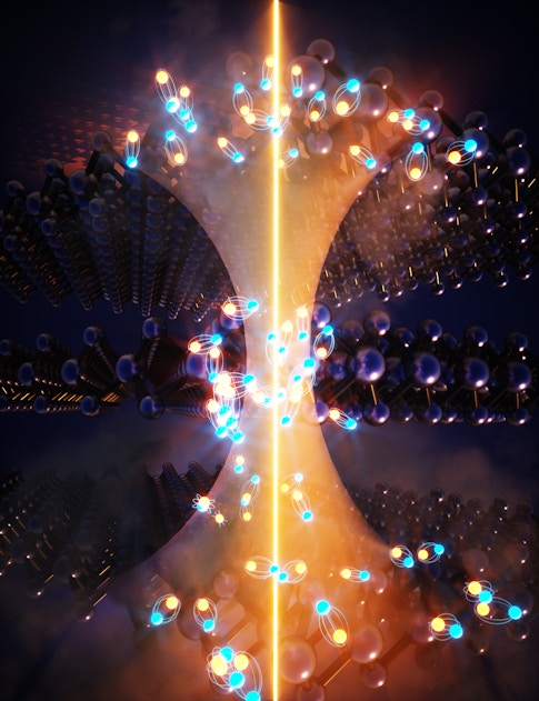
Nature sets a limit on how tightly light can be focused. Even in microscopes, two different objects that are closer than this limit would appear to be one. But within a special class of layered crystalline materials — known as van der Waals crystals — these rules can sometimes be broken. In these special cases, light can be confined without any limit in these materials, making it possible to clearly see even the smallest objects.
In their experiments, the researchers studied the van der Waals crystal called tungsten diselenide, which is of high interest for its potential integration in electronic and photonic technologies because of its unique structure and strong interactions with light.
When the scientists illuminated the crystal with a pulse of light, they changed the crystal’s electronic structure. The new structure created by the optical-switching event allowed something very uncommon to occur: The dispersion became ‘hyperbolic,’ confining light to a very small scale in one direction while allowing propagation in another. One potential application of this setup is the ability to image super-fine details on the nanoscale.
More generally, the work provides a new method for optical manipulation on the nanoscale. This research area, called nanophotonics, has become critical for researchers seeking ways to meet the increasing demand for technologies that go beyond what is possible with conventional photonics and electronics.
Dmitri Basov, Higgins professor of physics at Columbia University and senior author of the paper, believes the team’s findings will spark new areas of research in quantum matter.
“Laser pulses allowed us to create a new electronic state in this prototypical semiconductor, if only for a few picoseconds,” he says. “This discovery puts us on track toward optically programmable quantum phases in new materials.”


