Controlling the Complexity: Tuning Quantum Materials for Science and Technology

One day, Sophie Beck hopes to look at a phone, solar panel or other electronic device and be able to point to a specific technological advancement in that device that emerged from the field of strongly correlated materials, the focus of her research. Beck, a materials scientist at the Flatiron Institute’s Center for Computational Quantum Physics (CCQ), develops and uses novel computer simulation methods to study how electron interactions shape materials properties. Prior to arriving at CCQ in 2020, she earned a doctorate in materials science from ETH Zurich and a master’s degree in physics from the University of Freiburg in Germany. Beck’s approach forms the basis for predicting new materials and studying their properties, which could one day make our electronic devices more energy efficient.
Beck recently spoke to the Simons Foundation about her work and the future of technology. The conversation has been edited for clarity.
What area of materials science do you work on?
I am interested in a group of materials that are described as ‘strongly correlated’ and whose properties are often more complex and intriguing than those of conventional semiconductors. Scientists are interested in strongly correlated materials because their electronic and magnetic properties are often sensitive to small external changes — such as temperature or pressure — that could become control knobs for next-generation technologies. The electronic structure of correlated materials is largely determined by electrons confined to localized orbitals — meaning the spatial region in which electrons can move is limited. Examples of such materials are transition metal oxides. These are compounds in which an ion from the transition metal row of the periodic table, such as vanadium or copper, is combined with other ions such as oxygen that are electrically inert in this context. This configuration forces the electrons to interact much more strongly than in other types of materials
One example of a change in electronic structure is the metal-insulator transition, in which a material switches between a metallic state, which conducts electrical charge well, and an insulating state, in which conductivity is limited. In conventional semiconductor-based metal-insulator transition system such as a transistor, the switching is accomplished by moving electrons into and out of the device. In strongly correlated systems the transition is caused by changing the electronic state, without moving charge over large distances. Electronic devices based on strongly correlated materials may therefore be more efficient and higher-performing than conventional transistors.
Another advantageous aspect of these materials is that they can be stacked and even combined, much like Lego bricks. This flexibility leads to the idea of a ‘materials-by-design’ principle, where we could ideally create artificially engineered compositions of functional materials with desired properties. But this requires a comprehensive understanding of the electronic structure of these materials under various conditions. We do this using computational materials modeling.
What approaches do you use to do this modeling?
To understand the fundamental electronic properties of a solid, materials scientists typically use what we call ab initio simulations. A widely used approach to such simulations treats the interacting electrons as effectively independent. However, in strongly correlated systems, this assumption breaks down and we need a more sophisticated set of computational tools. Essentially, we need to find a way to model the dynamics of all of the electrons at once which has led to the emergence of an entire field of development of physical theories, mathematical tools and computational algorithms.
This often requires bringing together people from different disciplines. Recently, I have been working closely with applied mathematician Jason Kaye, also at the Flatiron Institute, to improve the accuracy of electronic transport calculations, which quantify how well a material conducts electricity. Identifying materials with promising transport behavior, whether highly conducting or even superconducting, requires reliable and robust methods, and our need for such predictions seems to grow steadily.
Are computer simulations more useful than experiments for understanding electron transport?
Both the experimental and theoretical angles have different advantages and limitations, so they should be combined to form a coherent picture. Experiments are often the first to reveal interesting phenomena, but sometimes the understanding that can be achieved at the experimental level is limited. For example, if one is interested in the electronic transport behavior of a material and discovers something surprising, it can be challenging to determine the exact physical origin of that signal since it may result from a sum of different factors. Atomic simulations can fill that gap because we can more easily investigate the factors that may play a role independently, which is not necessarily possible in an experimental setup.
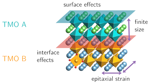
An example is a study we did on a strongly correlated metal called calcium vanadate (CaVO3). It was known from experiments that thin films of this material become insulating when the thickness is reduced to a few atomic layers, but in the experiment at that time it was not possible to distinguish whether this effect was due to the finite thickness of the film, the strain on the sample, the surface of the film, or the interface to the material it is grown on. Using electronic structure calculations, we were able to explore the possible options one by one to disentangle the complex interplay and improve our understanding of such phenomena. The computational approach also allows us to test new ideas with comparatively little effort, which can lead to exciting material predictions.
How does your research help in advancing next-generation technologies?
Materials scientists like myself sometimes think about what types of next-generation materials we could create that can be used to improve technology. In my field of research, we try to lay the groundwork for understanding the fundamentals of these materials and discovering interesting properties that engineers can translate into actual devices. The metal-insulator transition is a good example because it could help us build improved solar cells that can harvest energy from different wavelengths of light from the sun more efficiently, or electronic devices such as transistors that are more energy-efficient.
It would be fantastic if one day, eventually, some of the advances we are making now could be routinely used in next-generation technology. In the meantime, that also makes it exciting when I read an interesting new paper and wonder if it might be considered a seminal work for a new field or technology in 10 or 20 years.